RT9490 Application Note
Abstract
In portable device applications, the RT9490 is useful for battery charging. Usually, devices use RT9490 to stop charging. This application note provides the register control settings of RT9490 to stop charging by using battery pack back-to-back MOSFET. Please note that users must follow this application note for charging process.
1.
Charging
System Structure
The general function block of charging system is shown in Figure 1. First, the host controls register settings of the RT9490 for charge profile. The main duty of the RT9490 is to complete charge cycle with the charge profile and to inform the host of the charge status. The gauge device in the battery pack controls the back-to-back MOSFET to charge and discharge. The host communicates with the RT9490 and the gauge via the I2C interface.
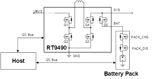
Figure 1. FunctionBlock of Charging System
2.
Charging
Behavior When Battery Pack Stops Charging
Figure 2 shows the charging behavior in the condition where battery pack stops charging. When the charging current is stopped by PACK_CHG MOSFET turn- off, RT9490 Q5 turns off after charging is done. After Q5 turns off, the voltage on RT9490 VBAT is below the battery voltage with forward diode VF, which triggers re-charge to turn on Q5 again. In Figure 3, when Q5 turns on and enters Q5 forced-on mode, without charging current, the converter target is VBAT tracking mode. Therefore, the converter stops switching until VBAT/VSYS OVP is triggered.
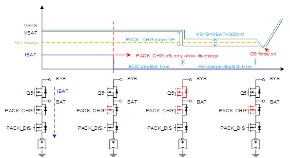
Figure 2. Charging Behavior When Battery Pack Stops Charging (not scaled)
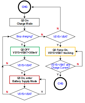
Figure 3. RT9490 Converter Behavior
3.
Charging
Behavior with RT9490 Software Workaround
As shown in Figure 2, the RT9490 stops switching until VBAT/VSYS OVP. To prevent triggering this protection, the host must set the RT9490 registers step by step. The programming steps are shown as below:
1. Write REG0xF1 = 0x69, hidden mode pass code.
2. Write REG0xF2 = 0x96, hidden mode pass code.
3. Write REG0x6F[5] = 0, disable BAT tracking mode.
4. Write REG0xF1 = 0x00, exit hidden mode.
5. Write REG0xF2 = 0x00, exit hidden mode.
After the above register setting is done, the converter behavior is shown in Figure 4.
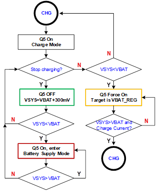
Figure 4. RT9490 Converter Behavior with Software Workaround
4.
Experiment
Waveform with the Software Workaround
Test Condition: VBAT_REG = 9.06V, battery pack OVP = 9.06V, trigger pack OVP protection to turn off the charging path. In Figure 5, the converter works in BAT tracking mode, VSYS/VBAT rise until triggering RT9490 VSYS/VBAT OVP protection.
In contrast, in Figure 6, the converter works with the software workaround by disabling BAT tracking mode. VSYS/VBAT rise to VBAT_REG to trigger “charge done”, and then VBAT falls to trigger “re-charge”. This cycle keeps looping for normal charging process.
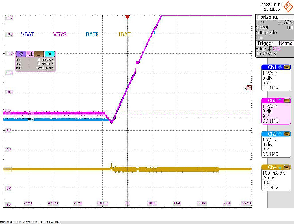
Figure 5. PACK_CHG off, without Software Workaround
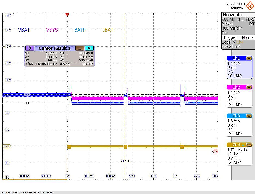
Figure 6. PACK_CHG off, with Software Workaround
5.
Appendix
Register Description
I2C Slave Address: 1010011 (53H)
R/W: Read and write
RWC: Read and write, also automatically cleared by particular conditions
Register Address: 0xF1, Register Name: TM_PAS_CODE1
|
Bit
|
Bit Name
|
Default
|
WDT RST
|
REG RST
|
Type
|
Description
|
|
7:0
|
TM_PAS_CODE1
|
00000000
|
N
|
Y
|
RWC
|
Passcode 1 for hidden mode
|
Register Address: 0xF2, Register Name: TM_PAS_CODE2
|
Bit
|
Bit Name
|
Default
|
WDT RST
|
REG RST
|
Type
|
Description
|
|
7:0
|
TM_PAS_CODE2
|
00000000
|
N
|
Y
|
RWC
|
Passcode 2 for hidden mode
|
Register Address: 0x6F, Register Name: HD_ADD_CTRL 2
|
Bit
|
Bit Name
|
Default
|
WDT RST
|
REG RST
|
Type
|
Description
|
|
5
|
EN_FON_Q5_BAT_TRACK
|
1
|
N
|
Y
|
R/W
|
0: When Q5 is forced on, no BAT tracking
1: When Q5 is forced on, BAT tracking
|